Light exposure
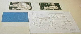 |
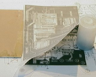
On this picture you can see both sheets with the layout and
the double-sided PCB to the left. I always use PCBs from Bungard,
because they have a constant high quality.
|
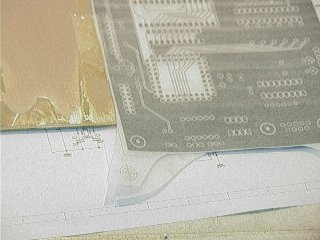
When making a single-sided PCB remove the protective film and place the layout
with two strips of adhesive tape with the printed side on the PCB. With
double-sided PCBs the case is a bit more difficult. The main problem is that
both sheets must be positioned accurately, so top and bottom layer are correctly
aligned. For this you simply use a piece of PCB material to which both sheets are
positioned. Attach the first sheet to the piece with adhesive tape. Now position
the second sheet on top of the piece and align the most remote point of the
sheets. Then use the adhesive tape to fixate the top sheet.
|
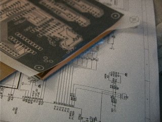
After that place the PCB in the pocket between the two sheets (remove the
protective foils prior to doing this) and tape down the sheets with adhesive
tape on both sides on the PCB. Necause the sheets are now fixated, the piece
of PCB-material can be removed.
|
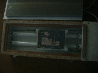
Now the PCB is exposed to UV-light. For this I have built an exposure unit, whose electronic
parts (UV-fluorescent tubes, sockets and starter) can be bought in electronics shops as kit,
you only have to build a box for it. Pay attention to the cover of the box, it must be covered
by a plastic foam which presses the PCB flat to the glass plate to ensure sharp edges of the
tracks.
The exposure time has to be found out experimentally. With PCBs from Bungard this isn't very
critical, about 2.5 to 3.5 minutes.
|